2024.12.10 | EPI Solution
EpiSolution utilizes a highly controlled zinc (Zn) diffusion process to form p-type regions in InP-based epitaxial wafers. This technique is essential for fabricating high-performance III-V devices such as photodiodes, laser diodes, and integrated optoelectronic components. Our Zn diffusion process ensures excellent reproducibility, uniformity, and electrical performance across the wafer.
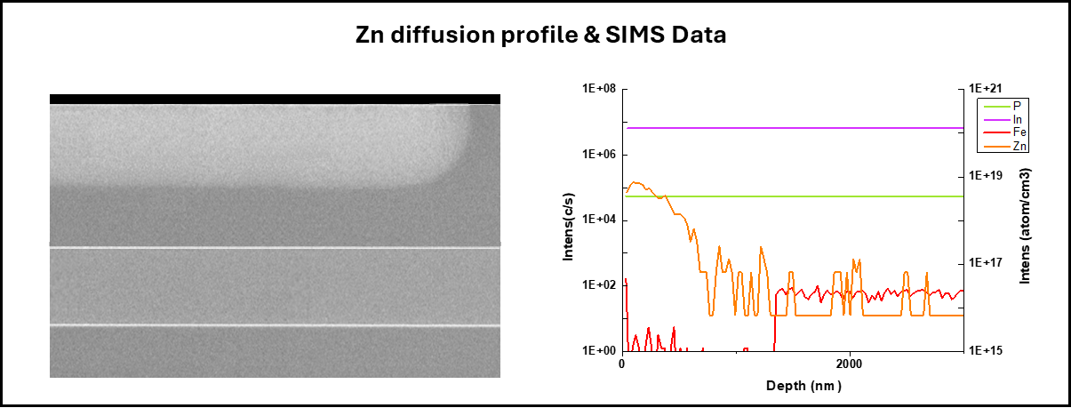
Zn diffusion is a thermal doping method where zinc atoms are diffused into the top surface of the epitaxial layer to create a p-type region. By carefully engineering the diffusion depth and profile, EpiSolution achieves low-leakage p-n junctions with precise control of carrier concentration.
Our Zn diffusion process is fully compatible with MOCVD-grown PIN and APD structures and is supported by a suite of advanced processing techniques: