2024.12.10 | EPI Solution
A PIN photodiode consists of p+, intrinsic, and n+ layers.
The wide intrinsic layer reduces junction capacitance and increases the depletion width, enabling faster response and better performance.
A built-in electric field across the intrinsic layer aids in efficient charge carrier separation.
InGaAs PIN photodiodes stand out in the near-infrared (NIR) spectrum for their excellent sensitivity, minimal dark current, and rapid response speed.
Unlike traditional silicon detectors, InGaAs materials maintain high quantum efficiency and low noise across the 900–1700 nm wavelength range. Furthermore, these diodes exhibit consistent performance across a broad range of temperatures while maintaining linearity and requiring low power input.
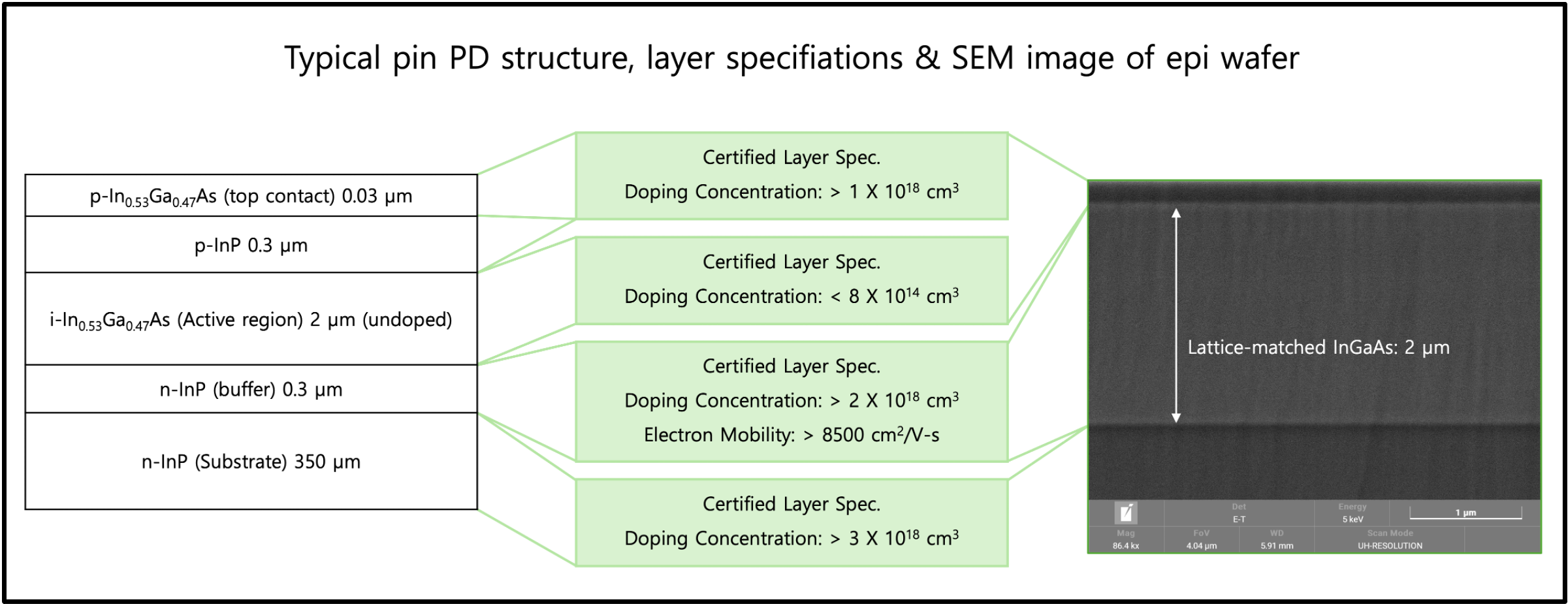
Our In0.53Ga0.47As epi wafer, lattice-matched to InP, is engineered for high-performance photodetector applications. Manufactured via MOCVD, it offers excellent material quality and uniformity across 2–4 inch wafer sizes. With a background carrier concentration below 8×10¹⁴ cm⁻³ and carrier mobility over 8,500 cm²/Vs, this structure ensures low dark current, high sensitivity, and reliable device performance. Rapid diode prototyping with available I-V and PL data makes it ideal for telecom, industrial, and medical applications.
Episolution has been developing MOCVD Zn-diffused structures on epi wafers with a focus on high-quality fabrication. To achieve excellent epi wafer quality and device performance, the company applies a variety of advanced process techniques, including lift-off contact ring formation, PECVD SiO₂ deposition, and SiO₂ RIE etching. These processes enable precise layer control, reliable surface passivation, and excellent interface uniformity, which are essential for high-performance optoelectronic device manufacturing.