Research-grade epitaxial wafers


Selective Area Regrowth for Buried Heterostructure (BH)

2024.12.10 | EPI Solution


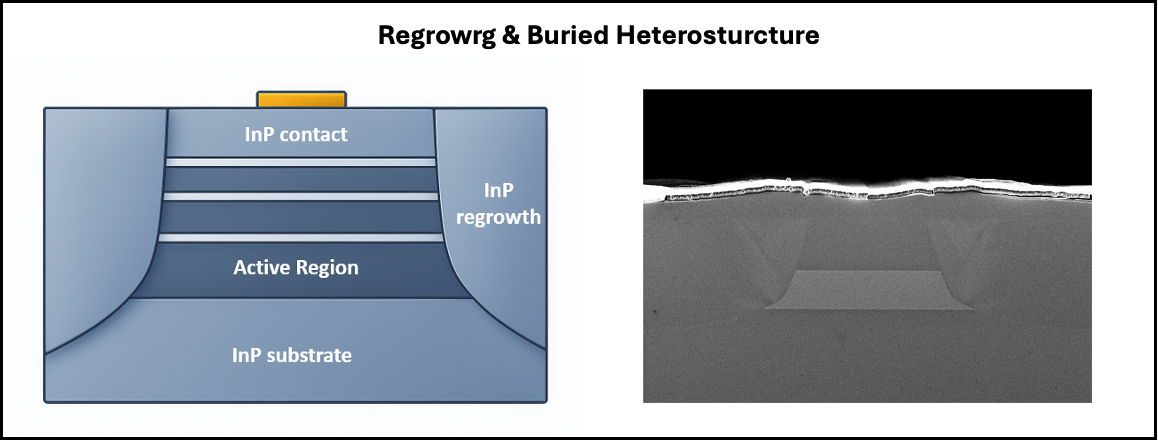
EpiSolution offers advanced Selective Area Regrowth technology for the formation of Buried Heterostructure(BH), a critical process step for high-performance III-V optoelectronic devices. This technique enables precise lateral and vertical confinement of both current and optical modes by embedding the active region with selectively regrown insulating or semi-insulating layers. Unlike conventional growth methods, Selective Area Regrowth allows for localized epitaxial regrowth only in predefined openings, significantly improving current blocking, noise suppression, and thermal stability across a wide range of device applications, including photodetectors, modulators, and integrated photonic components.


Performance Highlights

  • Selective Mask Patterning and Opening Definition
    • PECVD-deposited SiO₂ or SiN masking
    • RIE (Reactive Ion Etching) used to open well-defined regrowth windows
  • Regrowth of Fe-doped or Semi-Insulating InP Layers
    • Lateral current blocking and optical confinement
    • Formation of buried structures for enhanced isolation and device reliability
  • Pre-regrowth Surface Treatment
    • In-situ thermal desorption and pre-flow steps to minimize interface defects
    • Ensures atomically clean surfaces for high-quality epitaxial interfaces
  • Atomically Smooth Regrowth Interface
    • RMS roughness < 5 Å confirmed via AFM and TEM


Key Specifications

  • Substrate: InP (2-inch)
  • Regrowth Materials: Fe-doped InP, Semi-insulating InP
  • Masking Layer: PECVD SiO₂ or SiN
  • Interface Roughness: < 5 Å RMS
  • Regrowth Uniformity: < ±3% across wafer
  • Growth Method: MOCVD-based Selective Regrowth Process