Research-grade epitaxial wafers


TCAD Simulation Service

2024.12.10 | EPI Solution


EpiSolution provides advanced TCAD (Technology Computer-Aided Design) simulation services for semiconductor device design and optimization. Our solutions allow researchers and engineers to virtually prototype complex device structures before fabrication, reducing development cost and accelerating time-to-market.


Comprehensive Simulation Capabilities

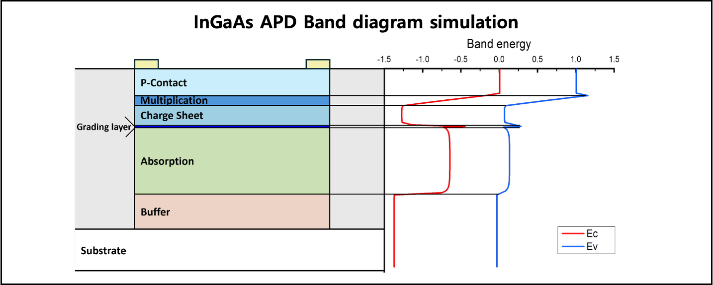
We deliver accurate modeling and numerical analysis across a wide range of semiconductor devices, including:

  • Band Diagram Analysis: visualize energy band alignment, heterojunction interfaces, and quantum well confinement effects
  • Electric Field Distribution: evaluate breakdown voltage, carrier drift dynamics, and avalanche multiplication regions
  • Doping Concentration Profiles: simulate dopant diffusion, activation, and junction depth with nanometer precision
  • Optical Absorption & Carrier Transport: model light–matter interaction for photodiodes, solar cells, and nanowire devices
  • Thermal Effects & Reliability: predict self-heating, leakage, and long-term stability under high-power operation


Why Choose EpiSolution’s TCAD Simulation?

  • Tailored to Epitaxial Structures: optimized for InGaAs PIN PDs, APDs, QCLs, and GaAs solar cells, reflecting our unique expertise in epitaxy and superlattice design
  • Accelerated Device Development: test multiple design iterations virtually before moving into costly wafer growth and processing
  • Seamless Integration with Fabrication: simulation parameters aligned with our MOCVD-grown epitaxial wafers for maximum consistency between theory and practice

Applications

  • High-speed InGaAs photodetectors (PIN PD, APD, SPAD)
  • Quantum Cascade Lasers (QCLs) with custom superlattice designs
  • GaAs high-efficiency solar cells for aerospace and IoT applications
  • Custom Device Requests