2024.12.10 | EPI Solution
EpiSolution has demonstrated the catalyst-free, self-assembled growth of InAsP nanowire arrays directly on Si (111) substrates using industry-compatible photolithography. This breakthrough enables scalable III–V integration on Si for high-mobility transistors, infrared photodetectors, and future nanoscale optoelectronic systems.
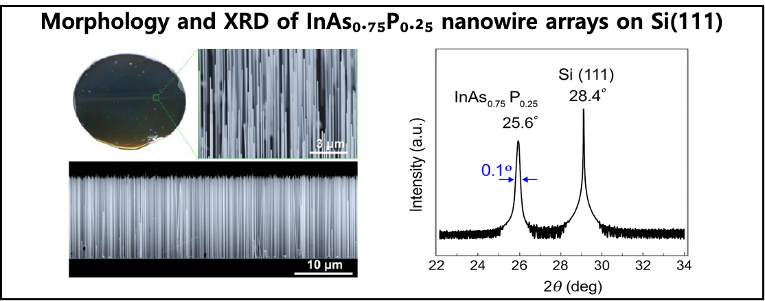
Unlike traditional vapor–liquid–solid (VLS) growth, our technique avoids metal catalysts such as Au, thereby eliminating contamination risks that degrade device performance. Instead, we achieve direct InAs heteroepitaxy through a Volmer–Weber growth mechanism, supported by poly(L-lysine) surface treatment that enhances nucleation selectivity and array uniformity.
This innovation bridges III–V materials and Si platforms, paving the way for high-performance nanowire-based FETs, photodetectors, and quantum devices.