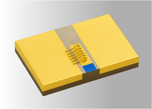
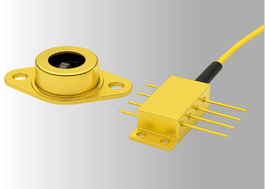
EPISolution delivers epitaxial wafers from research-grade to premium quality, leveraging proprietary superlattice design and advanced epitaxial growth to achieve atomic-level precision. With continuous innovation and research, we drive the advancement of semiconductor and optoelectronic materials.
EPI Solution’s QCL technology, built on proprietary superlattice design, delivers precision, power, and tunability in the mid-infrared spectrum. It enables advanced sensing, secure communications, and defense applications. With nanometer-scale growth control and proven reliability, we set new performance standards for next-generation optoelectronic systems.
Our InGaAs-based SPAD technology delivers exceptional sensitivity, low noise, and fast timing in the near-infrared spectrum, enabling quantum communication, high-resolution LIDAR, advanced defense systems, and biomedical imaging. With precision epitaxial growth, optimized device processing, and rigorous characterization, we provide reliable, application-tailored solutions for next-generation photodetection.