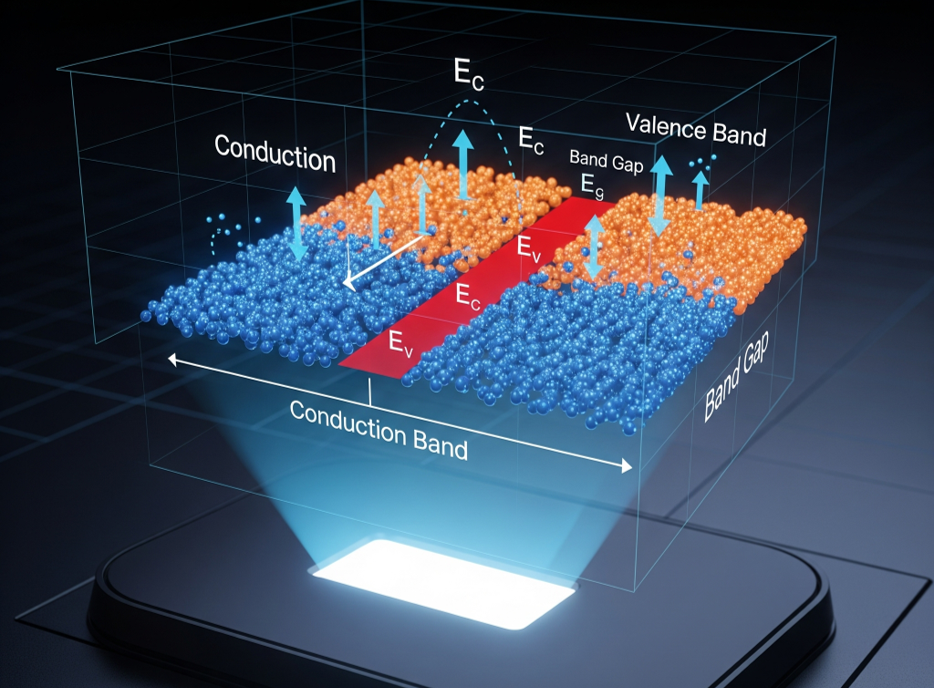
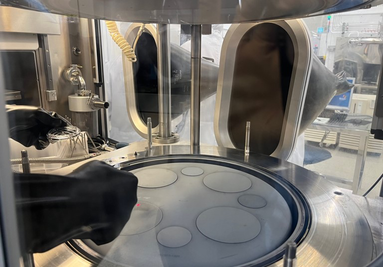
Epi Solution is a leading provider of InP-based III-V compound semiconductor technologies, with deep expertise in epitaxial growth, device fabrication, and advanced characterization.

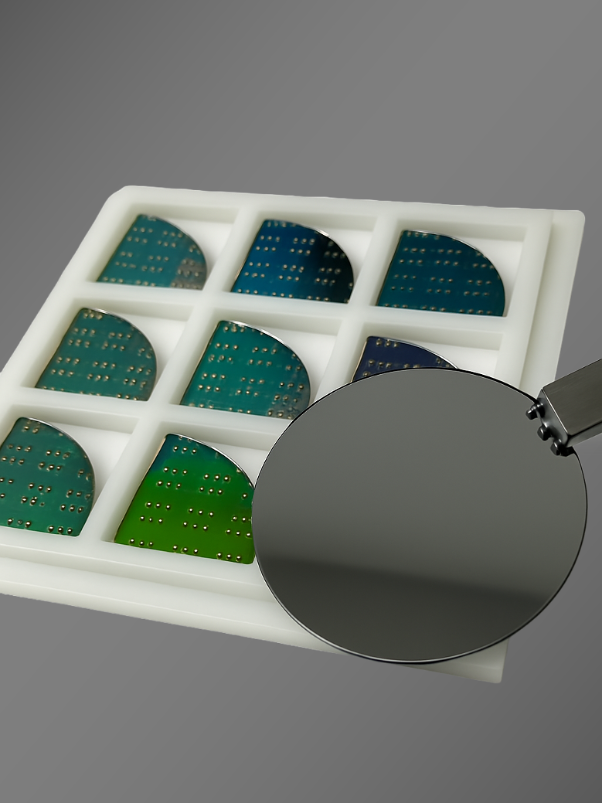
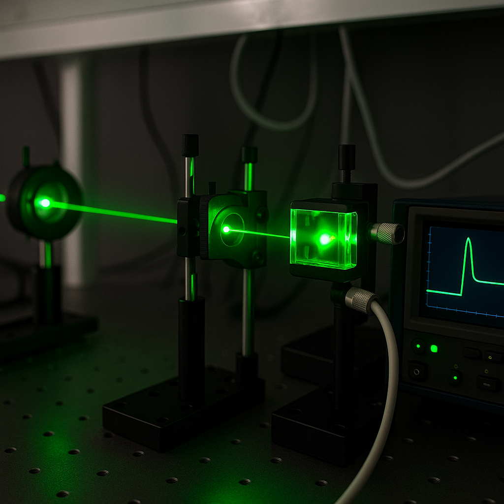
We are committed to supporting the advancement of photonic and electronic devices by providing high-quality, research-grade epitaxial wafers at affordable prices—enabling universities, research institutes, and startups to accelerate their innovation in III-V semiconductor technologies. Through customizable, high-performance epitaxial solutions, we aim to serve as the foundational enabler of breakthroughs in quantum sensing, high-speed communication, infrared imaging, and next-generation optoelectronics.

Simultation

Simulation

TCAD-based simulation of optoelectronic devices, including near-infrared laser diodes, quantum cascade lasers, InGaAs-based PIN photodiodes and avalanche photodiodes (APDs), and solar cells.

Epitaxy

Epitaxy

Advanced epitaxial growth technology for InP-based III-V compound semiconductor structures.

Fabrication

Fabrication

Fabrication of a broad range of III-V compound semiconductor optoelectronic devices, including laser diodes, photodetectors, and solar cells.

Measurements

Measurements

Comprehensive electrical and optical characterization in the near- and far-infrared spectral regions.

Customer Reviews


Who We Are

At Epi Solution, we lead InP based III–V compound semiconductor innovation through deep expertise in epitaxial growth.

We deliver ultra pure, highly uniform heterostructures with atomic level control, providing the material foundation for next-generation photonic and electronic devices. Our proprietary superlattice know-how and precisely optimized processes protect material integrity, reproducibility, and yield across every wafer. Guided by precise metrology and strict quality criteria, we consistently meet and exceed demanding specifications and help turn ambitious device concepts into production-ready epitaxy.

We understand that the success of advanced technologies depends on material integrity, and our processes are meticulously optimized to meet—and exceed—the most stringent industry standards.

Driven by innovation and commitment to excellence, we offer customized epitaxial solutions tailored to the unique design needs of each client.

Sincerely,
The Epi Solution Team

Our Vision (more)

  • Lead InP based epitaxy innovation
  • Advance fabrication capabilities for high performance applications
  • Deliver precision characterization across the full infrared spectrum

Our Mission (more)

  • Advancing epitaxial wafer technology for cutting-edge applications
  • Enabling far-IR quantum sensing, single-photon detection, and high-speed communication

What We do (more)

  • Research-Grade Epitaxial Wafers
  • Premium-Grade Epitaxial Wafers
  • Single Photon Avalanche Photodetector(SPAD)
  • TCAD simulation

Latest News

에피솔루션, ‘제31회 한국진공학회 반도체 및 박막분과 워크샵’ 공식 후원

차세대 화합물반도체 기술을 선도하는 에피솔루션(EpiSolution Co., Ltd.)이 오는 2025년 6월 26일부터 27일까지 GIST(광주과학기술원) 고등광기술연구원에서 개최되는 ‘제31회 한국진공학회 반도체 및 박막분과 워크샵’을 공식 후원한다.

Read More

에피솔루션 2025년 경기도 양자-반도체 융합산업 경쟁력 강화 사업 선정

㈜에피솔루션은 경기도 양자-반도체 융합 지원사업에 선정되어, 양자산업의 핵심 부품으로 꼽히는 InGaAs 기반 단일광자 검출기(SPAD)용 에피웨이퍼 국산화에 본격 착수했다.

Read More