2024.12.10 | EPI Solution
Our In₀.₅₃Ga₀.₄₇As avalanche photodiode (APD) epitaxial wafers are engineered for high-performance photon detection in the near-infrared (NIR) spectrum (900–1700 nm). These wafers are lattice-matched to InP substrates and grown via Metal-Organic Chemical Vapor Deposition (MOCVD), offering excellent uniformity, low dark current, and internal gain for enhanced signal detection.
InGaAs APDs extend the sensitivity of traditional photodiodes by incorporating avalanche multiplication, enabling detection of extremely weak optical signals. The internal gain mechanism amplifies the photocurrent, improving signal-to-noise performance and making them ideal for time-of-flight measurements, quantum communication, and long-range optical sensing.
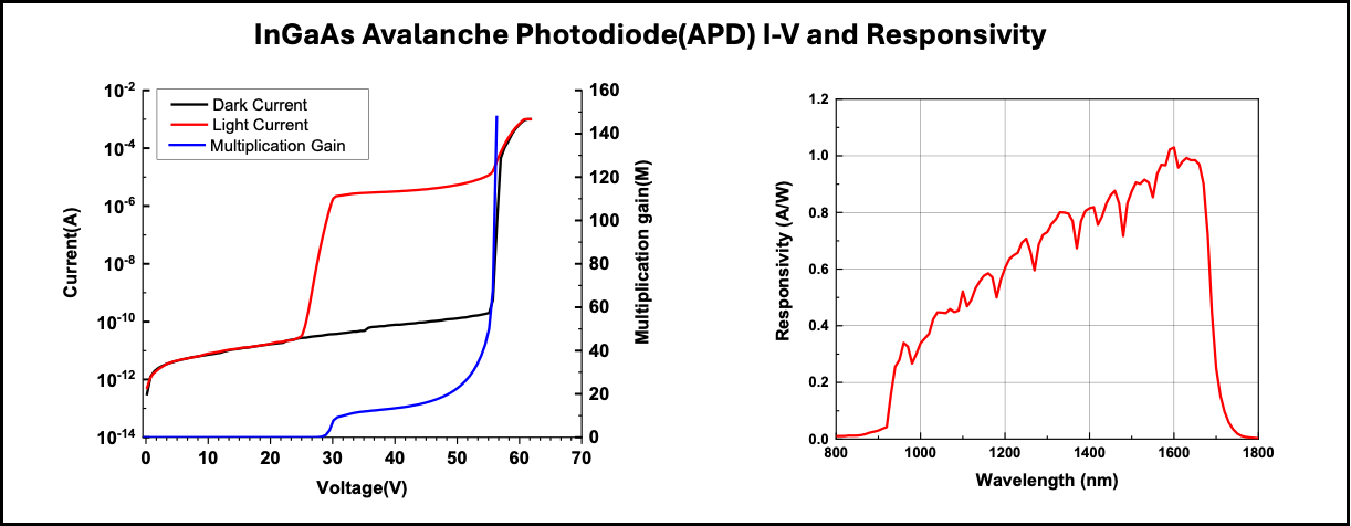
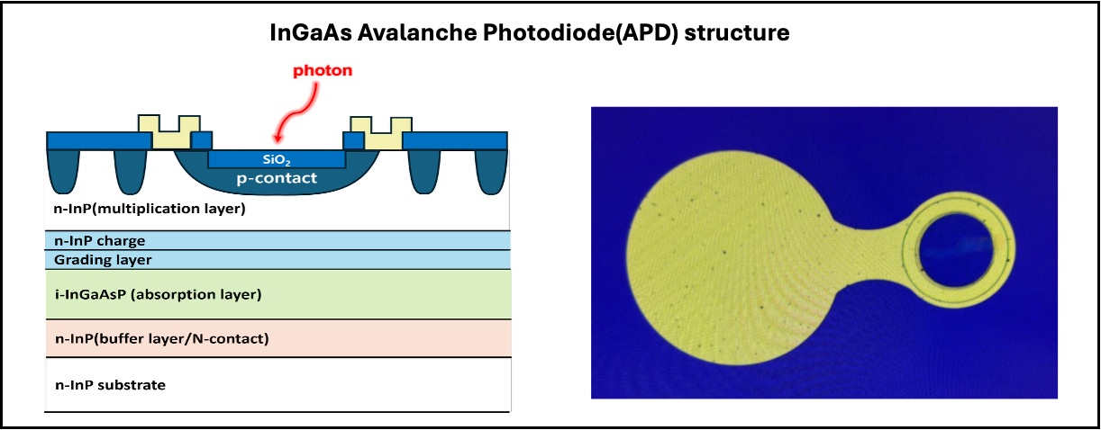
EpiSolution’s InGaAs APDs adopt the Separate Absorption and Multiplication (SAM) structure, integrating a carefully engineered grading layer between the absorption (InGaAs) and multiplication (InP) regions. This grading layer mitigates hole accumulation at the valence band barrier—an issue commonly observed in conventional SAM structures—by smoothing the bandgap transition. As a result, carrier transport is significantly improved, avalanche gain is enhanced, and excess noise is reduced, enabling high responsivity and stable operation even under high bias conditions.
Our APD wafers are fabricated using advanced MOCVD growth techniques with sub-5% layer thickness variation and interface roughness under 5 Å RMS (verified via TEM/AFM). We offer process compatibility with passivation, Zn-diffusion for junction formation, and lift-off techniques, ensuring reliable device prototyping and manufacturing.